- 您现在的位置:买卖IC网 > Sheet目录369 > W9751G6IB-25 (Winbond Electronics)IC DDR2-800 SDRAM 512MB 84-WBGA
�� �
�
�W9751G6IB�
�7.3�
�7.3.1�
�Command� Function�
�Bank� Activate� Command�
�(� CS� =� "L",� RAS� =� "L",� CAS� =� "H",� WE� =� "H",� BA0,� BA1� =� Bank,� A0� to� A12� be� row� address)�
�The� Bank� Activate� command� must� be� applied� before� any� Read� or� Write� operation� can� be� executed.�
�Immediately� after� the� bank� active� command,� the� DDR2� SDRAM� can� accept� a� read� or� write� command�
�on� the� following� clock� cycle.� If� a� Read/Write� command� is� issued� to� a� bank� that� has� not� satisfied� the�
�t� RCDmin� specification,� then� additive� latency� must� be� programmed� into� the� device� to� delay� when� the�
�Read/Write� command� is� internally� issued� to� the� device.� The� additive� latency� value� must� be� chosen� to�
�assure� t� RCDmin� is� satisfied.� Additive� latencies� of� 0,� 1,� 2,� 3� and� 4� are� supported.� Once� a� bank� has� been�
�activated� it� must� be� precharged� before� another� Bank� Activate� command� can� be� applied� to� the� same�
�bank.� The� bank� active� and� precharge� times� are� defined� as� t� RAS� and� t� RP� ,� respectively.� The� minimum�
�time� interval� between� successive� Bank� Activate� commands� to� the� same� bank� is� determined� by� the�
�RAS� cycle� time� of� the� device� (t� RC� ).� The� minimum� time� interval� between� Bank� Activate� commands� is�
�t� RRD� .�
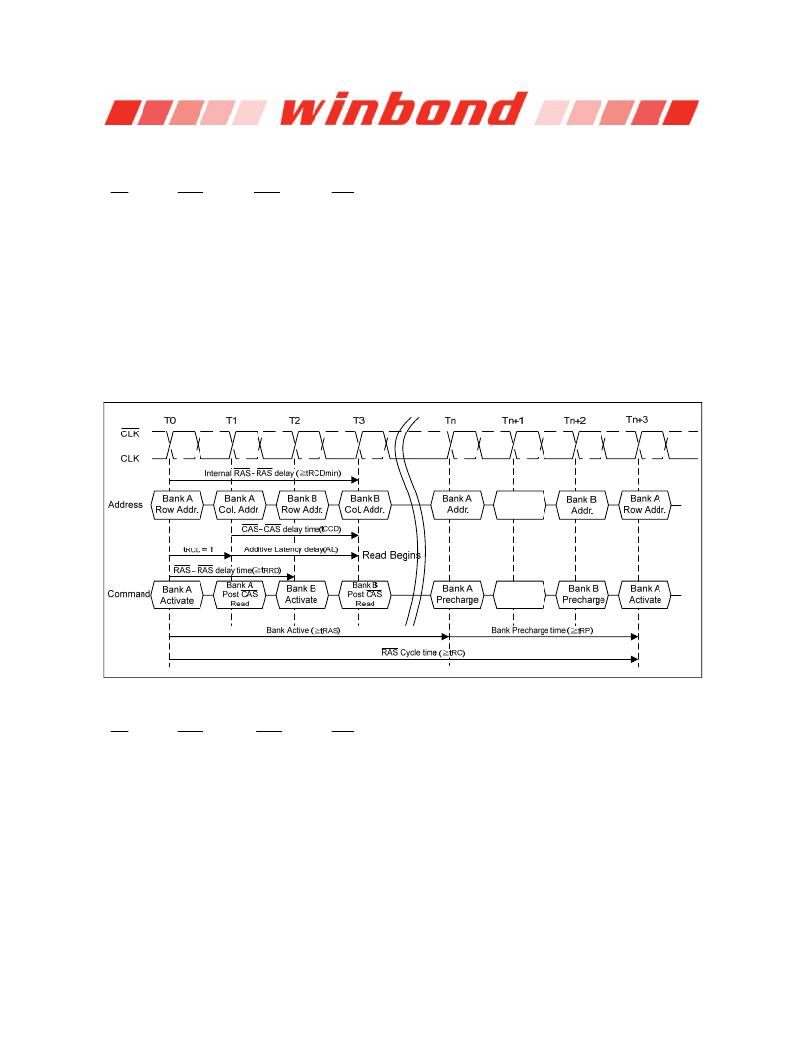
�Figure� 12� —� Bank� activate� command� cycle:� t� RCD� =� 3,� AL� =� 2,� t� RP� =� 3,� t� RRD� =� 2,� t� CCD� =� 2�
�7.3.2�
�Read� Command�
�(� CS� =� "L",� RAS� =� "H",� CAS� =� "L",� WE� =� "H",� BA0,� BA1� =� Bank,� A10� =� "L",� A0� to� A9� =� Column�
�Address)�
�The� READ� command� is� used� to� initiate� a� burst� read� access� to� an� active� row.� The� value� on� BA0,� BA1�
�inputs� selects� the� bank,� and� the� A0� to� A9� address� inputs� determine� the� starting� column� address.� The�
�address� input� A10� determines� whether� or� not� Auto-precharge� is� used.� If� Auto-precharge� is� selected,�
�the� row� being� accessed� will� be� precharged� at� the� end� of� the� READ� burst;� if� Auto-precharge� is� not�
�selected,� the� row� will� remain� open� for� subsequent� accesses.�
�Publication� Release� Date:� Oct.� 23,� 2009�
�-� 20� -�
�Revision� A06�
�发布紧急采购,3分钟左右您将得到回复。
相关PDF资料
W9751G6KB-25
IC DDR2 SDRAM 512MBIT 84WBGA
W9812G6JH-6I
IC SDRAM 128MBIT 54TSOPII
W9816G6IH-6I
IC SDRAM 16MBIT 50TSOPII
W9825G6JH-6I
IC SDRAM 256MBIT 54TSOPII
W9864G6JH-6I
IC SDRAM 64MBIT 54TSOPII
WM-5614
CABINET WALL MOUNT 37.25X17.9"
WRR-2244
RACK WALL MOUNT RELAY 42" X 19"
WRR-2264
RACK WALL MOUNT 75.25" X 19"
相关代理商/技术参数
W9751G6JB
制造商:WINBOND 制造商全称:Winbond 功能描述:8M ? 4 BANKS ? 16 BIT DDR2 SDRAM
W9751G6JB-25
制造商:Winbond Electronics Corp 功能描述:512GB DDRII
W9751G6JB-3
制造商:Winbond Electronics Corp 功能描述:512MB DDRII
W9751G6KB
制造商:WINBOND 制造商全称:Winbond 功能描述:8M ? 4 BANKS ? 16 BIT DDR2 SDRAM
W9751G6KB-18
制造商:Winbond Electronics Corp 功能描述:IC MEMORY
W9751G6KB-25
功能描述:IC DDR2 SDRAM 512MBIT 84WBGA RoHS:是 类别:集成电路 (IC) >> 存储器 系列:- 标准包装:1 系列:- 格式 - 存储器:闪存 存储器类型:闪存 - NAND 存储容量:4G(256M x 16) 速度:- 接口:并联 电源电压:2.7 V ~ 3.6 V 工作温度:0°C ~ 70°C 封装/外壳:48-TFSOP(0.724",18.40mm 宽) 供应商设备封装:48-TSOP I 包装:Digi-Reel® 其它名称:557-1461-6
W9751G6KB25A
制造商:WINBOND 制造商全称:Winbond 功能描述:Double Data Rate architecture: two data transfers per clock cycle
W9751G6KB25I
制造商:Winbond Electronics Corp 功能描述:DRAM Chip DDR2 SDRAM 512M-Bit 32Mx16 1.8V 84-Pin WBGA 制造商:Winbond Electronics Corp 功能描述:IC DDR2 SDRAM 512MBIT 2.5NS BGA